A published application is not a hand that was tested
On 8 October 2026 the U.S. Patent and Trademark Office published application US20260310299A1, “Three-Dimensional Soft Compliant Array Tactile Sensor with Multi-Modal Sensing and Scalable Manufacturing Methods.” The public-record mirror lists Tesla, Inc. as applicant and assignee, application 19/326,524 filed on 11 September 2025, and priority to provisional 63/783,580 filed on 4 April 2025. It lists 12 inventors with locations around Palo Alto, San Jose, Mountain View, Los Gatos, San Francisco and Gilroy. This check did not retrieve the USPTO PDF (HTTP 403). The mirror warns that some of its sections may be machine-processed. Identifiers and sentences below are from that mirror until the PDF is checked. [1] [2]
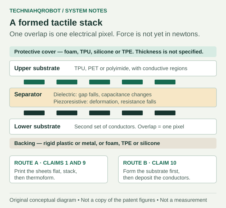
The mirror text contains 20 claims. Three are independent. Claim 1 is a method: define conductors on a first substrate, place a separator between that substrate and a second substrate that already has conductors, then form the stack into a target three-dimensional shape. Claim 10 is a different method: form the first substrate to the target shape before the conductors are defined. Claim 19 is a sensor, not a method. It requires two substrate layers, conductors, a separator that isolates the two conductor sets, and a stack that “is thermoformed” to the target shape. Claim 20 says the separator is either a dielectric material or a piezoresistive material. [1]
FIG. 1 is an example of a robotic hand. Sensor 102A lies along the thumb and follows the thumb’s geometry. Sensor 102B sits on the palm and can cover a substantial part of that surface. Sensor 102C sits on the index finger. The same paragraph says further sensors of this kind can go on any part of the hand, and that the sensors may be used on other surfaces. Three patches in a figure do not describe a complete five-finger product, and they do not identify which hand, if any, is in production. [1]
Flat taxels miss contact that lands on a curve
The background states the limitation the applicants chose to write down. A rigid, flat tactile sensor does not follow a curved or irregular surface, so sensitivity falls or contact is missed. On a finger, contact is not confined to a flat pad. An object can meet the pulp, the side of a digit or the palm. If the sensor cannot sit on that surface, the load passes through a gap, a wrinkle or a hard edge. The application’s answer is a soft stack formed to the target geometry, with regions that can be read separately. [1]
That instrument is not an optical fingertip. An optical taxel images the deformation of a gel or membrane with a camera inside the finger. Sideways motion of an internal pattern can show shear and incipient slip. The filing read here does not describe a camera, a marker pattern, shear, slip or temperature. It describes a change in capacitance or resistance when force deforms a separator. Read the optical guide when the question is how a camera inside a fingertip sees deformation. Read this filing when the question is how a formed film might cover a thumb, a palm and a finger with printed or deposited electrodes. [1]
For the camera-in-the-fingertip case, use the existing guide. How optical tactile sensors help robotic hands
An overlap of two conductors is one pixel
The application calls each independently readable region a “pixel.” In the manufacturing description, a pixel is a portion of the conductors on the two substrates that overlap, with the separator between them. FIG. 4D shows one sheet carrying parallel traces. The text says any number and any pattern of conductors may be used, chosen for a target spatial resolution that is never given as a number. It does not, in the passages read, require the second sheet to run at a right angle to the first, and it does not publish a row count or a column count. Treating the film as a conventional row-column matrix is an inference, not a claim. [1]
Capacitive separator: distance changes the reading
If the separator is a compliant dielectric, the application says an applied force compresses it, the conductors move closer, and the capacitance changes. External readout circuitry on the conductors detects that change. For an ideal parallel-plate capacitor, capacitance is C = εA/d: permittivity of the gap, times plate area, divided by separation. If ε and A stay fixed, a smaller d raises C. A formed tactile stack is not that ideal capacitor. The electrodes are traces, not full plates. Compression is local. Forming can change area and thickness. The filing states the distance effect. It does not publish ε, A, d, or a plot of capacitance against force. The formula explains the direction of the effect. It is not a calibration from the application. [1] [3]
Piezoresistive separator: deformation lowers resistance
If the separator is piezoresistive, the application says force deforms it and the resistance between the conductors decreases. Example materials are carbon-loaded silicone, conductive elastomers and conductive foams. The separator can be bonded by adhesive, lamination or thermal bonding. No resistance-versus-force table is included. Claim 20 allows one of the two separator types. It does not describe one installed film that reports capacitance and resistance as two simultaneous channels. [1]
The title says “multi-modal.” In the text that was read, the two modes are resistive sensing and capacitive sensing of surface force, touch and pressure. The text does not add a shear channel, a temperature channel or a proximity channel. A process that can build either electrical mode is not the same thing as one sensor that measures several physical quantities. Substrate examples in claim 2 are thermoplastic polyurethane, polyethylene terephthalate and polyimide. Screen-print inks named in the description include silver nanoparticle ink, silver-flake ink, carbon-based ink and copper-based ink. Another option cuts a channel with a laser, fills it with conductive paste, including a silver-derived paste, and laminates a cover that leaves pads exposed. [1]
The conductors leave the film through connectors. The description names zero-insertion-force connectors, anisotropic conductive film, or solder to a flexible printed circuit board. The backing behind the film can be rigid plastic or metal, or a soft foam, thermoplastic elastomer or silicone, attached by adhesive, overmolding or fasteners. A protective layer in front can be foam, thermoplastic polyurethane, silicone or thermoplastic elastomer, at a uniform or variable thickness. The application says that layer can block moisture, dust and abrasion, and that it should be chosen so the sensor stays compliant. It may also be opened in places for electrical contact. It does not give a thickness, a hardness, or a measurement of how far the cover spreads a point load across neighboring pixels. A thick soft cover can raise two pixels when the object touched one spot. That blur is a design variable, and the filing leaves it open. [1]
Print flat and then form, or form first and then print
The two independent methods are two orders of work. They are not two names for one production line. Route A starts flat. Route B starts with the curved substrate. The apparatus claim does not automatically swallow both. [1]
| Question | Stated in the application | Not stated |
|---|---|---|
| Route A, claims 1 and 9 | Define conductors on flat sheets, stack the separator, then thermoform the stack in a mold. | Stretch of the traces, change in resistance, and electrode misalignment after forming. |
| Route B, claims 10 to 17 | Form the first substrate, then deposit conductors by 3D dispensing, laser activation plus plating, or pad printing. Dispense or laminate the separator. | Placement error, minimum bend radius, and parts per hour on a compound curve. |
| Apparatus, claim 19 | A stack of two conductor-bearing substrates and a separator that is thermoformed to the target shape. | A sensor made only by depositing conductors on an already formed shell. That sequence sits in the method claims. |
| Electrical mode, claim 20 | Separator is a dielectric or a piezoresistive material. | A force curve, a pixel pitch, and a second physical channel such as shear or temperature. |
FIG. 6 shows the thermoforming arrangement used after the stack exists: a heater, a mold whose surface is the target contour, and optional positive air pressure on the stack. The description says the stack is heated to a glass-transition temperature, pressed to the mold, cooled, and then holds the shape. The first sheet may be cut with alignment holes, channels or notches so the two conductor sets can be registered. The text says the conductors are aligned so that overlaps become the pixels. It does not give a misalignment budget. Heating a printed stack until the polymer softens can move ink, thin a trace on an outside bend, and shift one electrode set relative to the other. The filing describes the sequence. It does not report that those defects were measured, or that they were avoided. [1]
Route B avoids stretching a finished electrode pattern across a mold. It asks a different process question: whether a dispenser, a laser-plus-plate step, or a pad can hold trace width and position on a compound curve. Claim 12 is three-dimensional dispensing of conductive traces. Claims 13 and 14 activate a pattern with a laser and plate it. Claim 15 is pad printing. Claim 16 dispenses the separator onto those conductors. Claim 17 couples a dielectric layer instead. Claim 18 mounts a backing. None of those claims includes a tolerance. [1]
Claim 19 is narrower than the union of the methods. Its stack “is thermoformed.” A film built only by writing conductors onto a pre-formed shell is described, if at all, by the method claims, not by the words of claim 19 as published. Collapsing “the patent” into one product specification hides that split. Injection molding and compression molding appear in the summary as other ways to reach a geometry. They are not the steps written into claims 9, 11 or 19. A sentence in the summary is not a claimed process. [1]
A changed pixel is not yet a grasp force
A grasp loop needs the contact location and a load the object and the hand can accept. A pixel in this filing can contribute only an electrical change at an overlap. If several overlaps on 102C change together, the index-finger patch was loaded somewhere in that group. If 102B changes and 102A does not, the palm patch was loaded and the thumb patch was not, within the limits of the cover and of electrical coupling the text never discusses. The application does not describe a shield between traces or a scan order. On a capacitive film, neighboring traces can couple even when only one overlap was compressed. Without a scan method, “which overlap changed” is not “which square millimetre was touched.” [1]
The signal is also not a force in newtons until it is calibrated on that geometry, with that cover, at that temperature, after forming. The filing does not provide the calibration. A rising capacitance, or a falling resistance, is evidence that the separator deformed. It is not, by itself, the normal force, the tangential force, or the start of slip. Slip is tangential motion at the contact. A pressure-like reading can stay high while the object slides. It can also fall because the cover unloaded, or because the grip opened. Those cases are not separated by one electrical number. [1] [3]
A six-axis sensor at the wrist estimates the net load on the hand and can be calibrated in newtons and newton-metres. It cannot tell a palm contact from a fingertip contact when both produce the same net wrench. A distributed film can separate those surfaces and still fail to give a reliable net force. A program that needs both the contact patch and the load needs both measurements, or an explicit decision that one of them is out of scope. This application does not discuss a wrist sensor. It should not be read as a replacement for one. [1]
Contact sensing sits after pose and reach. How humanoid robots pick up objectsThe filing covers the film, not the rest of that sequence.
When the filing is useful, and what to ask for next
Use the document as a process description with a boundary around missing measurements. It is relevant when the design problem is coverage of a curved thumb, palm or finger by a film whose electrodes are printed or deposited and then read as many overlaps. It is not evidence that a named humanoid already carries that film, that the film survives a shift of work, or that a controller can servo grip force from the raw reading. [1]
- Pixel pitch, and the number of independently wired overlaps on one finger and on one palm. “Any number” is not a wiring plan.
- A plot of electrical output against normal force, before forming and after forming, with the protective cover installed.
- For route A, the change in trace resistance and the electrode misalignment caused by one thermoforming cycle. For route B, the placement error of dispensing, plating or pad printing on the target curve.
- A contact task on a stated hand: object, hardware version, trial count, and failures, published separately from the patent text.
Until those records exist, the statement that matches the evidence is narrow. Tesla is the applicant on a 20-claim application for forming a soft capacitive or resistive array into a three-dimensional shape. The example geometry includes a robotic thumb, palm and index finger. The publication does not establish that any particular robot uses the film, how fine the pixels are, or how a grasp controller should turn the electrical change into a force. [1] [2]
Sources and verification
- US20260310299A1, three-dimensional soft compliant array tactile sensor ↗Public-record mirror of the USPTO application · Read 12 October 2026
Specification, 20 claims, abstract and bibliographic block read on 12 October 2026. The mirror says some sections of its site may be machine-processed and that the USPTO record controls. Publication data as reproduced there: US20260310299A1, application 19/326,524, filed 11 September 2025, priority to provisional 63/783,580 filed 4 April 2025, published 8 October 2026. Applicant and assignee listed as Tesla, Inc. Inventor name spellings are not repeated here.
- USPTO publication PDF address for US20260310299A1 ↗United States Patent and Trademark Office · Read 12 October 2026
Official PDF address associated with the 8 October 2026 publication. This check received HTTP 403 and did not retrieve the file. Mirror wording should be confirmed on that PDF before a sentence is treated as final.
- Parallel plate capacitor ↗HyperPhysics, Georgia State University · Read 12 October 2026
Ideal relation C = εA/d for two plates. Used only to interpret a change in separation. It is not a calibration of the sensor in the application.
Evidence limits
- The USPTO PDF returned HTTP 403. The mirror warns that some of its text may be machine-processed, so sentence-level wording still needs that PDF.
- No pixel pitch, force curve, sample rate or cycle life appears in the application text that was read.
- The text does not name Optimus and does not report a robot trial.
- Claim 19 requires a thermoformed stack and should not be merged with every method claim.
- Cover thickness and electrode stretch after forming are undescribed, so spatial accuracy is unknown.
Article history
Added a claim-level reading of US20260310299A1, separating the two forming routes, the capacitive and resistive separators, and the robot results the application does not contain.
Report a correction